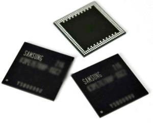
 Samsung has started making flash storage chips that it claims will be twice as fast and up to 10 times more durable than the current flash storage used in mobile devices.
The so-called V-NAND flash memory employs a 3D structure in which storage modules are stacked vertically, said Steve Weinger, director of NAND marketing at Samsung Semiconductor, a division of Samsung.
Samsung is already producing the new flash chips in volume and has shipped units to companies for qualification and testing. The technology will likely appear in enterprise solid-state drives this year and in mobile devices next year, Weinger said.
The 3D memory differs markedly from conventional NAND flash, in which storage modules are placed side by side. Samsung has stacked 24 NAND layers in one chip package, with each stack connected by a proprietary interconnect that Weinger described as the “secret sauce” that makes the 3D storage faster than conventional NAND.
The 3D stacking also helps build flash products with greater capacities, Weinger said. The initial products could be available with capacities ranging from 128GB to 1TB.
This is the first time that 3D stacking technology has been used in NAND flash, according to Weinger. Samsung is moving to a 3D design because placing NAND flash devices horizontally has become challenging with chip sizes shrinking, Weinger said.
The semiconductor industry has talked about chip stacking for years, and Samsung’s technology shows where the memory industry could be headed, said Dean McCarron, principal analyst at Mercury Research.
“If you’re trying to put a lot of stuff in a package, and you’re seeing the scaling laws of process technology coming to their limits, it makes sense to start stacking,” McCarron said.
Going vertical can help reduce the distance between components that need to communicate with each other, enabling rates of data transfers, he said.


